
TL;DR
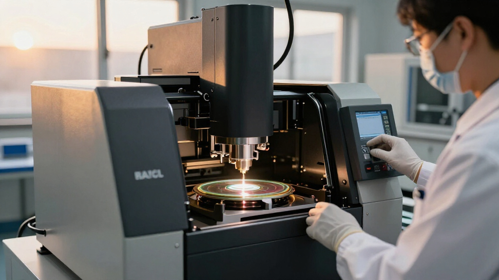
Intel has commenced shipping silicon wafers produced using high-NA EUV lithography. This development signals a major advance in semiconductor manufacturing, potentially enabling smaller, more powerful chips.
Intel has begun shipping silicon wafers manufactured with high-NA EUV lithography technology, marking a major milestone in the company’s advanced semiconductor manufacturing capabilities. This development confirms Intel’s progress in deploying next-generation lithography tools, which are critical for producing smaller, more powerful chips. The move is significant for the broader industry, as it demonstrates the commercial viability of high-NA EUV in high-volume production, potentially reshaping the chip supply chain and technological landscape.
Intel announced that it has started shipping silicon wafers produced using high-NA EUV (Extreme Ultraviolet) lithography, a technology that allows for more precise patterning at smaller nodes. The high-NA (Numerical Aperture) EUV tools are a step beyond standard EUV, offering higher resolution and enabling the production of chips with smaller features. The company did not specify the exact volume or the specific products but confirmed that the shipments are part of its ongoing efforts to integrate high-NA EUV into its manufacturing process.
This marks a significant milestone for Intel, which has been investing heavily in EUV technology over the past several years. The high-NA EUV equipment is supplied by ASML, a Dutch vendor that is the sole provider of EUV lithography tools with the high-NA capability. Industry analysts note that this move positions Intel to compete more effectively in advanced process nodes, potentially enabling next-generation CPUs and other high-performance chips.
Implications for Semiconductor Manufacturing Leadership
The shipping of high-NA EUV wafers by Intel signals a critical step toward mass production of chips at 5 nanometers and below. This technology is expected to enable smaller, faster, and more energy-efficient chips, which are vital for applications ranging from data centers to mobile devices. For Intel, this development could help regain ground in the competitive race against rivals like TSMC and Samsung, who are also advancing EUV capabilities. It may also influence supply chain dynamics, as high-NA EUV equipment is complex and costly, potentially creating new barriers for other players.
EUV lithography semiconductor equipment
As an affiliate, we earn on qualifying purchases.
As an affiliate, we earn on qualifying purchases.
Advances in EUV Lithography and Industry Timeline
High-NA EUV lithography has been in development for several years, with ASML unveiling its first high-NA EUV tools in 2021. These tools are designed to improve resolution by increasing the numerical aperture from 0.33 to 0.55, allowing for finer patterning. Industry leaders like TSMC and Samsung have been testing high-NA EUV, but widespread commercial deployment has been delayed by technical challenges and costs. Intel’s move to ship wafers indicates it has overcome some of these hurdles, although full-scale production remains a work in progress.
Previously, Intel primarily relied on standard EUV lithography for its advanced nodes, with plans to adopt high-NA EUV in its future process nodes. This shipping milestone confirms Intel’s progress in that direction, aligning with industry forecasts of high-NA EUV’s commercialization timeline.
“We are pleased to confirm that Intel has begun shipping silicon wafers produced with high-NA EUV technology, marking a significant step in our process roadmap.”
— Intel spokesperson
high-NA EUV lithography tools
As an affiliate, we earn on qualifying purchases.
As an affiliate, we earn on qualifying purchases.
Remaining Technical and Production Challenges
While Intel has begun shipping wafers with high-NA EUV, it is not yet clear how extensive the deployment will be across its product lines. Details about yield rates, cost implications, and the timeline for full-scale adoption are still emerging. Additionally, the industry continues to face challenges related to high-NA EUV’s complexity, including tool availability and process stability, which could influence the pace of broader implementation.
silicon wafer manufacturing equipment
As an affiliate, we earn on qualifying purchases.
As an affiliate, we earn on qualifying purchases.
Next Steps Toward Commercial High-NA EUV Adoption
Intel is expected to increase the volume of wafers produced with high-NA EUV and incorporate this technology into its upcoming process nodes, such as Intel 20A and beyond. Industry watchers will monitor for updates on yield improvements, product launches, and whether other manufacturers follow suit. The next major milestone will likely involve Intel’s announcement of products utilizing high-NA EUV at commercial scale, possibly within the next 12-18 months.
advanced chip fabrication machinery
As an affiliate, we earn on qualifying purchases.
As an affiliate, we earn on qualifying purchases.
Key Questions
What is high-NA EUV lithography?
High-NA EUV lithography is an advanced chip manufacturing technology that uses extreme ultraviolet light with a higher numerical aperture to achieve finer patterning at smaller process nodes, enabling the production of smaller, more powerful chips.
Why is this development important for Intel?
Shipping wafers with high-NA EUV indicates Intel’s progress toward manufacturing at smaller nodes, which can lead to better performance and energy efficiency in its chips, helping it compete more effectively in the industry.
When will high-NA EUV be used in consumer products?
While Intel has begun shipping wafers, full-scale adoption in commercial products is likely within the next 12-18 months, depending on yield and process stability improvements.
How does high-NA EUV differ from standard EUV?
High-NA EUV offers higher resolution due to a larger numerical aperture, allowing for smaller feature sizes on chips compared to standard EUV tools, which are limited in their resolution capabilities.
Source: hn